Figure 2.
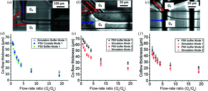
(a) Bright-field microscopy image of the T-junction geometry 3D-printed with IP-S photoresist in mode 1 with a flow-rate ratio of 1. (b) Bright-field microscopy image of the Y-junction geometry 3D-printed with IP-S photoresist in mode 2 with a flow-rate ratio of 4. (c) Bright-field microscopy image of the Y-junction geometry 3D-printed with PETA-B photoresist in mode 2 with a flow-rate ratio of 1. (d) Co-flow thickness of the T-junction device with PSII crystal in the buffer (filled green circles), PSII buffer only (filled blue triangles) and simulation (open blue triangles). The error bars indicate the standard deviation of the co-flow thickness. The devices used to test these conditions were made of IP-S photoresist. (e) The co-flow thickness of the Y-junction with PSII buffer in mode 1 (filled black circles) and mode 2 (filled red triangles) compared with the numerical simulation in mode 1 (open black circles) and simulation mode 2 (open red triangles). The error bars indicate the standard deviation of the co-flow thickness. The devices used to test these conditions were made of IP-S photoresist. (f) The co-flow thickness of the Y-junction with PSII buffer in mode 1 (filled black circles) and mode 2 (filled red triangles) compared with simulation mode 1 (open black circles) and simulation mode 2 (open red triangles). The error bars indicate the standard deviation of the co-flow thickness. The devices used to test these conditions were made of PETA-B photoresist.

