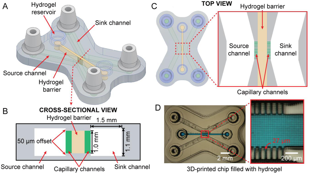
Fig. 2.
Structure of the 3D-printed hydrogel partitioning chip. (A) Oblique view of the 3D CAD design containing three channels: two flanking microfluidic channels (source and sink) and a central channel filled with a hydrogel barrier, connected to the source/sink channels via 27 μm-wide comb-like capillary channels. (B) Cross-sectional schematic of the 3D-printed chip; the capillary channels are depicted in green for clarity. (C) Top-view of the CAD design of the chip and a close-up view of the source/sink channels and the hydrogel barrier connected via capillary channels (green). (D) Micrograph of the 3D-printed hydrogel partitioning chip and a magnified image of the hydrogel barrier entrapped by the capillary channels. The hydrogel barrier channel is filled with blue dye for visualization purposes.

