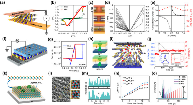
Fig. 4.
TMDs-based artificial synapse. a Vertical Cu/MoS2/Au memristors based on conductive filaments formation. b Typical I–V curve of resistive switching. c Schematics of the cumulative area change of Cu filaments causing LRS to HRS transition. d Bipolar and analog switching characteristic as an artificial synapse. e Demonstration of STDP behavior.
Reproduced with permission from Ref. [107]. Copyright 2019, Nano Letters. f Structure of Ag/ZrO2/WS2/Pt memristor device. g I − V characteristics of Ag/ZrO2/WS2/Pt heterostructure. h Schematic of the SET and RESET process. Reproduced with permission from Ref. [111]. Copyright 2019, American Chemical Society. i Illustration of the ion dynamics in Ag/SnS/Pt memristor. j Ultrafast switching curve of the device with 4 V/1.5 ns voltage pulse. Reproduced with permission from Ref. [140]. Copyright 2021, Nano Letters. k Schematic of Pd/WS2/Pt memristor operated by atomic-vacancy formation and migration. l TEM images of WS2 films in the LRS. m Line profile for W atoms; the upper (HRS) and lower images (LRS). n Pulse modulation by changing input voltage amplitude. o Response currents for pulse trains of 4 different frequencies (0.1, 0.2, 0.5, and 1 MHz). Reproduced with permission from Ref. [112]. Copyright 2019, Small (Color figure online)

