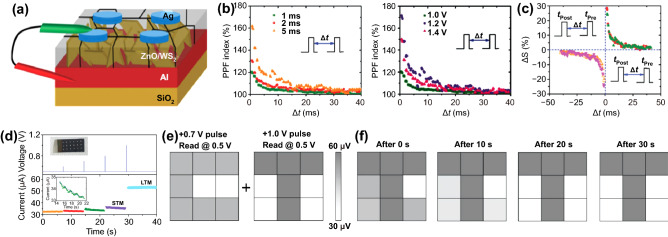
Fig. 6.
Memristor devices mediated by charge trapping and de-trapping. a Schematic structure of the Ag/ZnO/WS2/Al memristor. b PPF decays as a function of pulse interval (Δt) at different pulse amplitude and different pulse widths. c Experimental results for STDP. d The STM to LTM transition and the conductance variation by increasing input pulse voltage from + 0.7 to + 1.0 V. e Images of the letters “C” and “T” memorized in STM and LTM modes, respectively. f The measured current history of the 3 × 3 arrays from right after to 30 s after the written processes.
Reproduced with permission from Ref. [149]. Copyright 2019, Advanced Electronic Materials (Color figure online)

