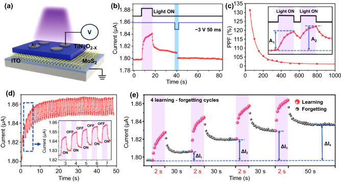
Fig. 8.
Combination of electric and photonic stimuli for demonstrating optoelectronic synaptic devices through Al/TiNxO2-x/MoS2/ITO heterostructures. a Schematic illustration of the device structure, b EPSC feature using photonic stimulus (3.15 mW cm−2, 10 s) and electrical erase with a voltage pulse (−3 V, 50 ms), and c light-induced EPSC-based PPF index. d The conductance changes under consecutive light pulses and e cyclic test to demonstrate the “learning–forgetting–relearning” process.
Reproduced with permission from Ref. [161]. Copyright 2021, Advanced Functional Materials (Color figure online)

