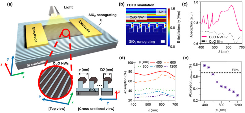
Figure 1.
Concept of the proposed high-performance visible light photodetector. (a) 3-D schematic of the proposed device. The device is composed of the perfectly aligned CuO nanowire array (see [Top view]) on the SiO2 nanograting substrate (see [Cross sectional view]). (b) FDTD simulation result of the proposed device (scale bar = 200 nm). (c) Calculated absorption of the 400 nm-pitch (p) of CuO nanowire (NW) array on SiO2 nanograting substrate (pink solid line). Black dashed line indicates the absorption of CuO thin film (thickness = 122 nm). Calculated absorption varying pitch of CuO NWs with same dimension on SiO2 nanograting from 400 to 1200 nm (width = 314 nm, thickness = 114 nm): (d) visible light range (λ = 400–700 nm) (e) λ = 550 nm.

