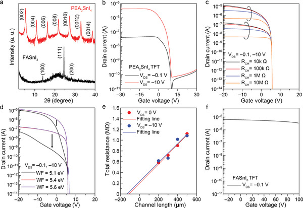
Figure 3.

TFT performances of 2D PEA2SnI4 and 3D FASnI3 TFTs. a) Comparison of the XRD patterns; b) transfer curve of 2D PEA2SnI4 TFT; device simulation results of the models for c) various series resistances in the channel layer and d) various Schottky barrier heights between the source/drain electrodes and active layer; e) total resistance of the 2D PEA2SnI4 active layer determined by the transmission line method; f) transfer curve of 3D FASnI3 TFT.
