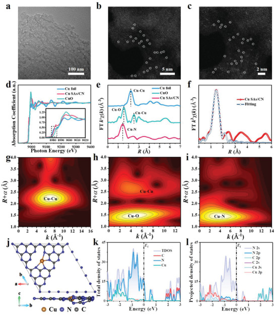
Figure 1.

Morphology, atomic structure characterization, and electronic structure analysis of Cu SAs/CN. a) TEM image. b,c) AC HAADF‐STEM images of Cu SAs/CN. The Cu single atoms are highlighted in white cycles. d) Normalized X‐ray absorption near‐edge structure (XANES) spectra of Cu foil, CuO, and Cu SAs/CN. Inset is the enlarged image of the dashed box. e) Fourier transform extended X‐ray absorption fine structure (EXAFS) spectra at the Cu K‐edge. f) The corresponding EXAFS fitting curves of Cu SAs/CN in R space. g–i) Wavelet transform (WT) spectra of Cu K‐edge for Cu foil, CuO, and Cu SAs/CN, respectively. j) The optimized unit structure of Cu SAs/CN (top view and side view). The blue, gray, and orange balls refer to the N, C, and Cu atoms, respectively. k) Total density states and orbital distribution of each element in Cu SAs/CN. l) Projected density states of Cu 3s, Cu 3p, C 2s, C 2p, N 2s, and N 2p orbital distribution.
