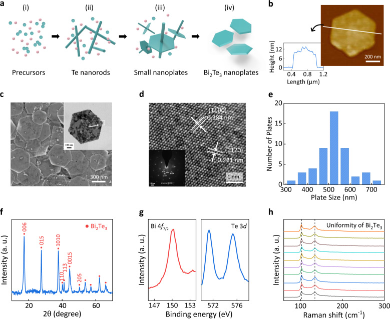
Fig. 1. Materials characterization of Bi2Te3 NPs.
a Schematic illustration of growth mechanism for Bi2Te3 NPs. b AFM image of a Bi2Te3 NP and the corresponding height/width profile along the solid line across the nanoplate. c SEM and TEM images (inset) of the hexagonal Bi2Te3 NPs. d HRTEM image of Bi2Te3 sample and the corresponding SAED image with bright hexagonally symmetric spots. e Statistic of the size distribution of Bi2Te3 NPs by AFM analysis. f XRD pattern of the fabricated Bi2Te3 NPs. g High-resolution XPS spectra of Bi 4f and Te 3d region, respectively. h Raman spectra were collected from stochastic sites on an individual Bi2Te3 NP. Source data are provided as a Source Data file.

