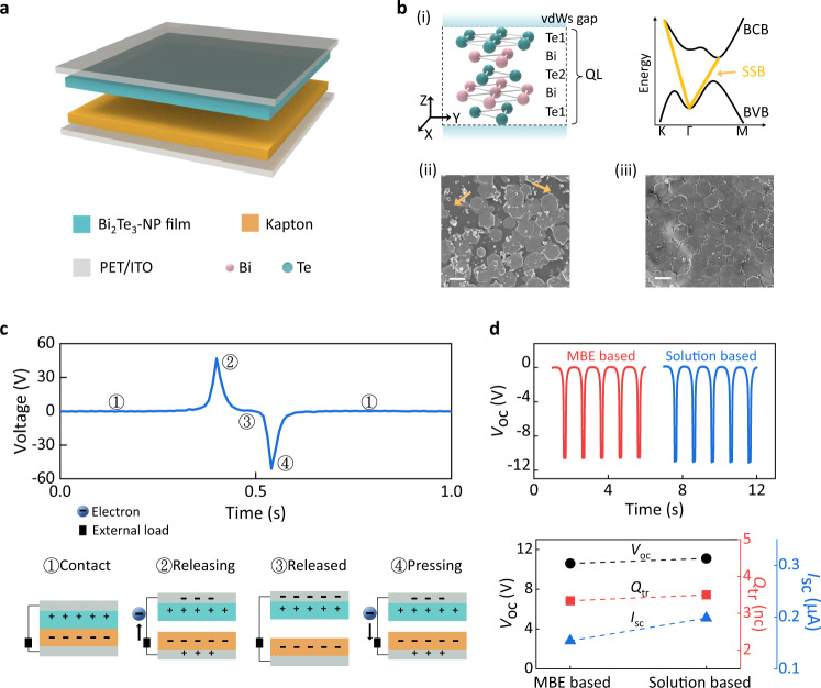
Fig. 2. The demonstration of the TI-TENG.
a Structural schematic diagram of a TI-TENG based on Bi2Te3-NP film. b Crystal structure (i) of the quintuple layer (QL) Bi2Te3 (Te(1)–Bi–Te(2)–Bi–Te(1)) and a sketch of the band structure diagram with typical bulk bandgap (bulk conductive band/BCB, bulk valance band/BVB, black lines) and unique conductive surface state band (yellow line, SSB). The vdWs gap represents the van der Waals gap between each QL. SEM images of the TI films with different coating doses of Bi2Te3 NP colloid ((ii) 2 mL and (iii) 10 mL). The scale bars are 500 nm and the arrows highlight the discontinuity of Bi2Te3-NP film with a lower coating dose. c Output voltage signal of solution-based TI-TENG (8 mL, 5 × 5 cm2) in one cycle. The down panels show the working principle for several different stages. d Comparison plots of the output properties of TI-TENGs assembled with solution-based Bi2Te3-NP film (8 mL, 0.5 cm2) and MBE-based Bi2Te3 film, which reveal their slight differences. Source data are provided as a Source Data file.

