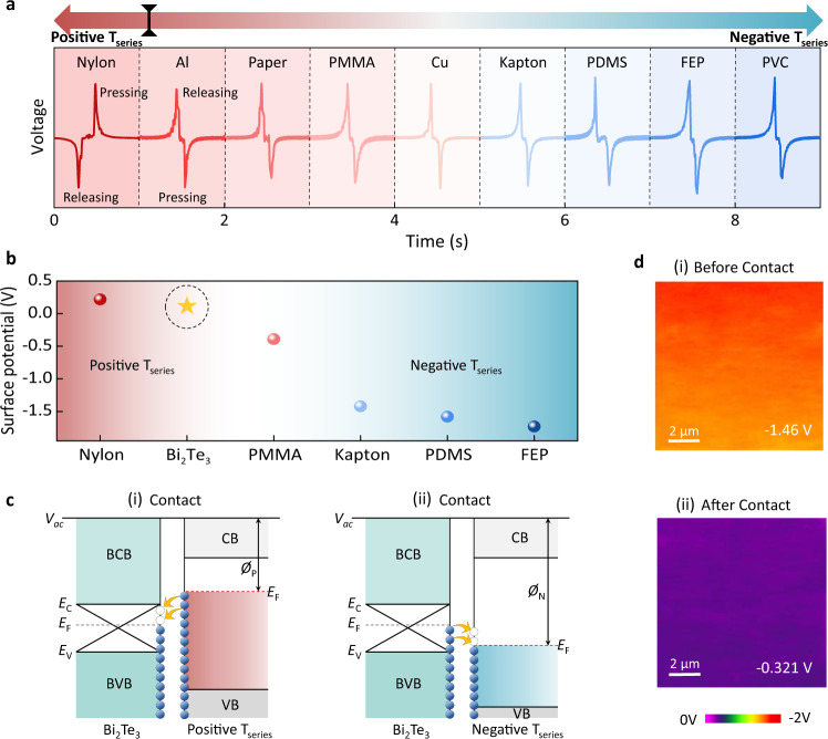
Fig. 3. Triboelectric series positioning of the TI films.
a Output signals of the solution-based TI-TENGs with various media as the counter triboelectric layer, which hint at the triboelectric series of TI film between nylon and Al film. Note that the red arrow indicates positively triboelectric (Tseries) charging properties and the blue arrow indicates negatively triboelectric charging properties. The black symbol on the arrow proposes the possible position of TI materials. b The measured surface potential of various triboelectric layers using the KPFM technique. The star symbol and the dashed circle denote the Bi2Te3-NP film. c Energy band diagram for Bi2Te3-NP film when contacting (i) positively electrified materials and (ii) negatively electrified materials. The crossed symbols indicate the conductive surface state of TI material. EF is the Fermi energy and Ec(v) is the bulk conductive (valence) band edge of Bi2Te3. Øp and Øn are the work functions for positive and negative triboelectric materials, respectively. d Surface potential variation of Kapton (i) before and (ii) after contact with Bi2Te3-NP film. Source data are provided as a Source Data file.

