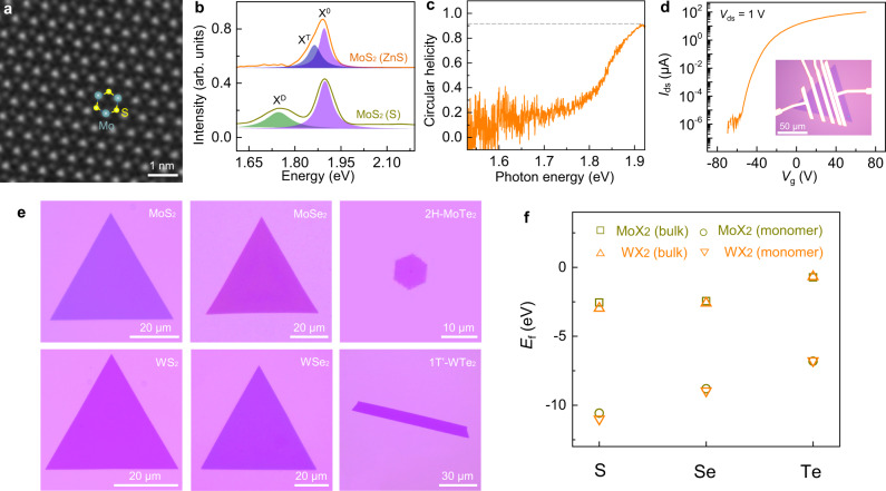
Fig. 2. Quality characterizations of the as-grown MoS2 domain and universal growth of diverse TMDs by chalcogen monomer supply.
a Atomic-resolved HAADF-STEM image of the prepared MoS2, revealing the high crystallinity of MoS2 without detectable S vacancies. b Low-temperature (10 K) PL spectra of MoS2 samples fed by S monomer (orange curve) and S powder (dark yellow curve), respectively. Three typical features, X0, XT, and XD peaks assign to neutral exciton, trion, and defect state emission peaks, respectively. The absence of XD peak confirmed the high quality of the MoS2 grown by S monomer supply. c The circular dichroism PL spectrum measured at 10 K. The near-unity polarization of MoS2 on sapphire indicates the high optical quality. The horizontal dashed line is added for clarity. d Transfer characteristic of the MoS2 FET with channel length and width of 7 μm and 22 μm, respectively, at a bias voltage Vds of 1 V. Inset: optical image of the device. e Optical images of the representative TMDs, including 2H phase MoS2, MoSe2, MoTe2, WS2, WSe2 and 1T′ phase WTe2. f The calculated formation energy (Ef) of the six representative TMDs. When chalcogen bulks are supplied as precursors, the formation of transition metal tellurides in relative to their corresponding sulfide and selenide are less favourable due to their high formation energies (−0.73 and −0.68 eV/unit for MoTe2 and WTe2, respectively). While it becomes highly favourable when Te monomers are applied.

