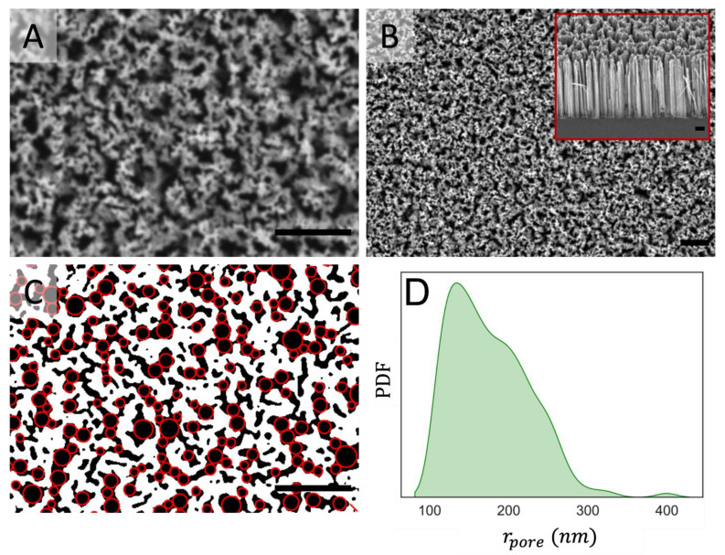
Figure 3.
Scanning electron microscopy (SEM) data for vertically aligned silicon nanowire arrays: (A,B) Top-view SEM images at different magnifications, inset in B displays SEM side view of the SiNW surface; (C) Representative segmentation mask generated from SEM images, showing silicon nano-wire arrays (white), pores (black) and inscribed circumferences (red) used to calculate the pore size; (D) Probability density function of the pore radius for SiNW surfaces weighted by the pore area. Scale bars are 2 µm.

