
Fig. 1.
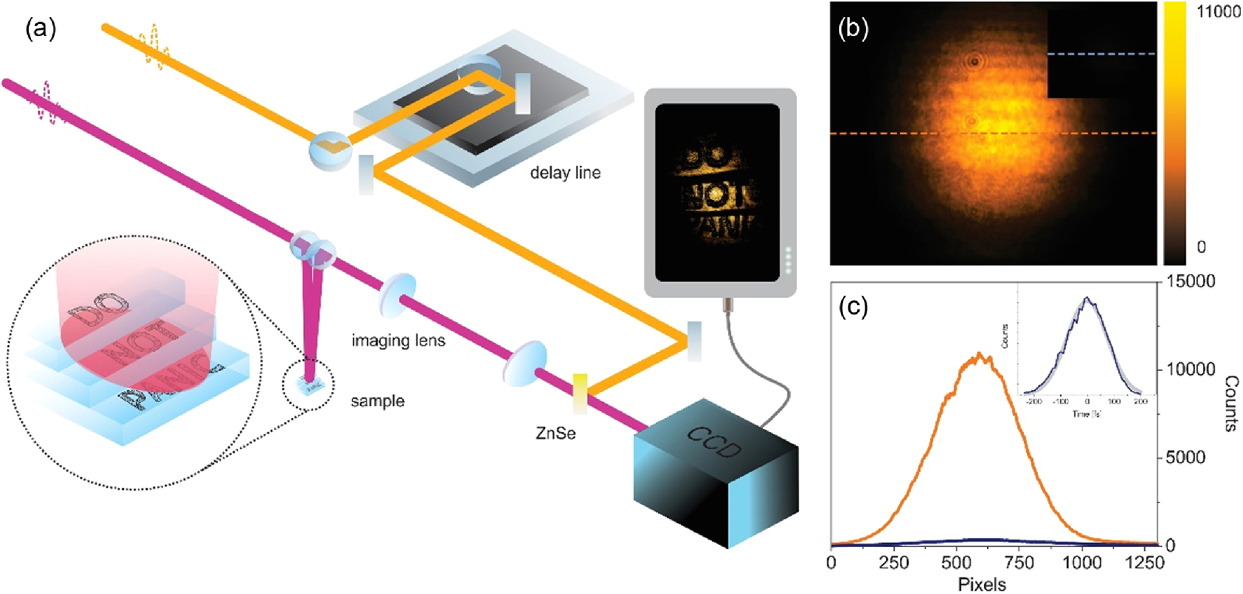
(a) Schematic representation of the setup. (b) Beam image on the CCD Si chip with MIR (2850 cm‒1, 3500 nm) and gate NIR pulses (8333 cm‒1, 1200 nm). The inset shows a gate pulse DTA image at the same scale. (c) Spatial cross section of the beam image on CCD Si chip with (NTA, orange line) and without MIR pulse (DTA, blue line). Inset: temporal cross-correlation of MIR and gate pulse, indicating a 110 fs pulse width (gray line—Gaussian fit).