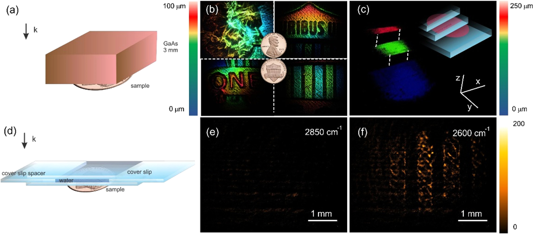
Fig. 3.

Sketch of penetration experiment arrangement through (a) 3 mm thick GaAs wafer and (d) 190 µm water layer. (b) 3D reconstruction of one cent US coin (Union Shield) through 3 mm GaAs wafer. (c) Tomographic imaging of stacked cellulose acetate sheets through 3 mm GaAs wafer. Imaging of one cent US coin (Union Shield) through 190 µm water layer (380 µm in double pass) at (e) 2850 cm‒1 and (f ) 2600 cm‒1.
