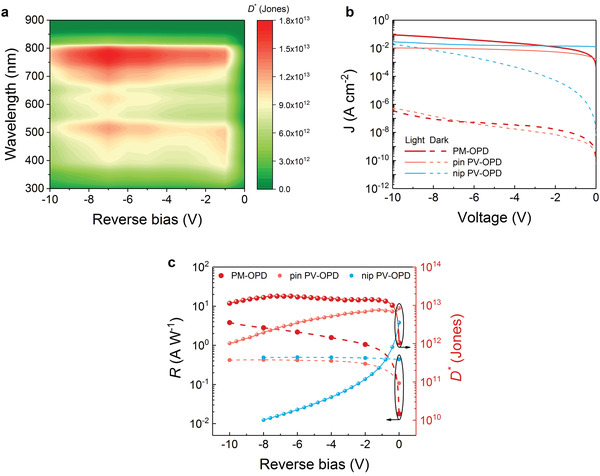
Figure 4.

a) Shot‐noise‐limited D * under reverse biases of the device comprising 4.0 wt% BDP‐OMe. b) J–V characteristics in the dark and under 100 mW cm–2 illumination of two different optimized PV‐OPDs (pin‐ and nip‐architecture) and optimized PM‐OPD. c) Comparison of the same devices shown in (b) in terms of R and D *. The R is calculated from the EQE measured at different voltages and fitted with a polynomial function at 780 nm, from which the D * is computed.
