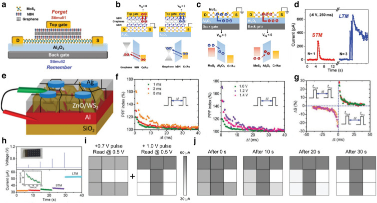
Fig. 6.
Memristor devices mediated by charge trapping and de-trapping. a The van der Waals heterostructure device composed of MoS2/hBN/graphene/hBN layers. b Illustration of volatile characteristics in top gate operation. c Illustration of nonvolatile characteristics in back gate operation. d Memory type transition from STM to LTM.
Reproduced with permission from Ref. [116]. Copyright 2019, Advanced Science. (Color figure online) e Schematic structure of the Ag/ZnO/WS2/Al memristor. f PPF decays as a function of pulse interval (Δt) at different pulse amplitude and different pulse widths. g Experimental results for STDP. h The STM to LTM transition and the conductance variation by increasing input pulse voltage from + 0.7 to + 1.0 V. i Images of the letters “C” and “T” memorized in STM and LTM mode respectively. j The measured current history of the 3 × 3 arrays from right after to 30 s after the written processes. Reproduced with permission from Ref. [149]. Copyright 2019, Advanced Electronic Materials. (Color figure online)

