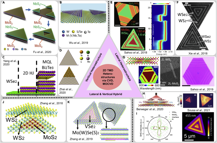
Figure 2.
A brief overview of the recent progress made toward CVD growth of TMD HSs, including vertical, lateral, and hybrid configurations.
(A) A proposed growth sequence of NbS2 on top of MoS2. NbS2 first nucleated at the corner on MoS2 and migrated at the edges having full coverage of the bottom layer of MoS2 (Fu et al., 2018). Copyright 2018, American Chemical Society.
(B) A schematic of a vertical MTe2 (M = V, Nb, Ta) on the WX2 (X = SE, S) layer (Wu et al., 2019c). Copyright 2019, Wiley.
(C) Schematic representation of multilayer Bi2Te3 on top of 1L-WSe2 (Yang et al., 2020). Copyright 2020, American Chemical Society.
(D) Atomic ball model for NiTe2/MoS2 vertical heterostructure synthesized via two-step CVD process (Zhai et al., 2020). Copyright 2020, American Chemical Society.
(E) Composite PL-map of three-junction MoS2-WS2 (top left) and five-junction of MoSe2-WSe2 (bottom left) lateral heterostructures. Normalized PL contour plot (colored) along a perpendicular to the interfaces corresponding to the three-junction MoS2-WS2 (Sahoo et al., 2018). Copyright 2018, Springer Nature.
(F) SEM images of WS2-WSe2 superlattices (Xie et al., 2018). Copyright 2018, AAAS.
(G) Schematic for bilayer lateral heterostructure (top left). A PL position mapping (bottom left) and HAADF-STM image (middle) corresponding to MoS2-WS2 bilayer lateral heterostructure. An optical image of bilayer multi-junction MoS2-WS2 lateral heterostructure is shown with the scale bar of 10 μm (Sahoo et al., 2019). Copyright 2019, American Chemical Society.
(H) Persistence photoconductivity mapping of WS2-MoS2 multi-junction lateral heterostructure (left), and (right) microwave real part of conductance signal (SG) of the channels with the increasing energy of excitation photon (1.75 and 1.97 eV) (Berweger et al., 2020). Copyright 2020, American Chemical Society.
(I) (left) Polarization dependence second harmonic generation (SHG) and (right) the corresponding SHG intensity maps of the single-layer MoSe2-WSe2 lateral heterojunction collected at 455 nm emission wavelength (Sousa et al., 2021). Copyright 2021, IOP.
(J) An atomic model of thin-film hybrid structure of WS2/WS2-MoS2 (Zhang et al., 2018). Copyright 2018, IOP.
(K) Schematic of VSe2 and TMDs hybrid structure where multilayer VSe2 was grown at the edges of 1L-TMDs followed by coverage of top layer via two-step CVD process (Zhang et al., 2019b). Copyright 2019, American Chemical Society.

