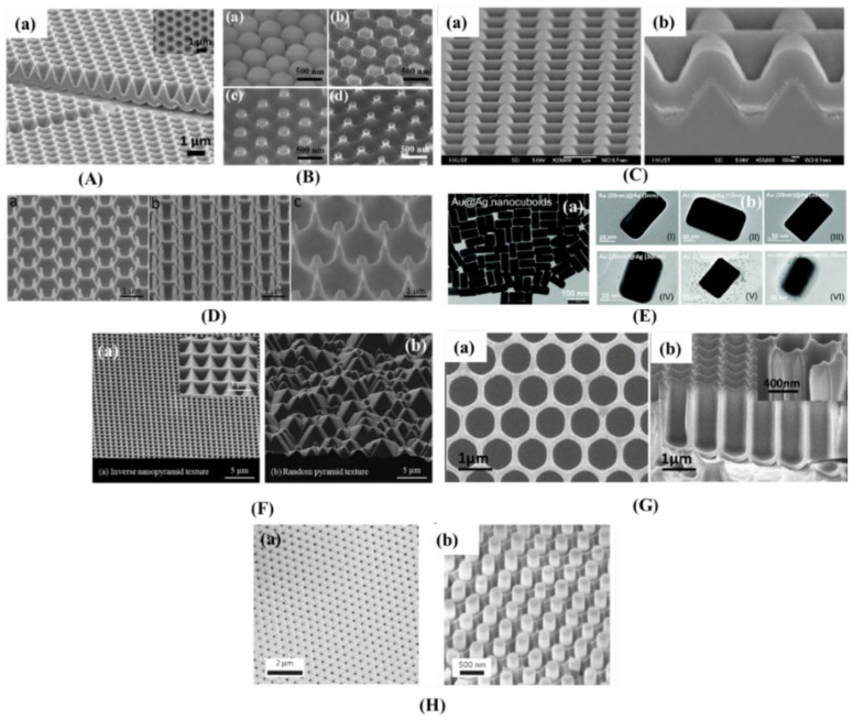
Figure 7.
(A). (a) SEM of Au nanocone-coated template with 1 µm pitch and 1 µm depth (reprinted with permission from [24], 2012, John Wiley and Sons). (B) SEM of a 500 nm polystyrene nanosphere monolayer and Si nanorod array. (C) SEM micrograph (75° angle) of an ultrathin a-Si/c-Si tandem solar cell on the top surface and at the cross-section (reprinted with permission from [24], 2012, Elsevier). (D) SEM view (60° angle) of nanopillar structures with different pitches and heights (a,b). Cross-sectional view SEM of integrated nanopillar/nanowell structures. (Reprinted with permission from [124], 2009, Springer Nature). (E). (a) TEM images of Au@Ag NCs and individual Au@Ag NCs with different Ag shell thicknesses along with an individual Au@Ag@SiO2 NC (reprinted with permission from [127], 2010, American Chemical Society). (F). SEM of surface textures showing 2D grating of an inverse nanopyramid pattern and the industry standard random pyramid texture (reprinted with permission from [128], 2012, American Chemical Society). (G). (a) Top view and cross-sectional view SEM of the nanowell sample. (H). (a) SEM of an as-made anodic alumina membrane (AAM) with perfectly ordered pores along with a CdS nanopillar array after partial etching of the AAM (reprinted with permission from [124], 2009, Springer Nature).

