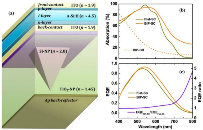
Figure 11.
(a) Schematic illustration of a BLiS back reflector for n–i–p Si thin-film solar cells. The TiO2 -NP layer over the planar silver back reflector had inverted pyramid-shaped microcavities, which were further covered by a flat-topped Si-NP layer. (b) Total optical absorption by Flat-SC and BIP-SC devices (solid lines) and parasitic absorption by the BIP-BR (dashed line). (c) Measured EQE (left-hand side y-axis) spectra of Flat-SC and BIP-SC devices and EQE ratio (right-hand side y-axis) [173]. Reprinted with permission from [173], 2020, Creative Commons Attribution License (https://creativecommons.org/licenses/by/4.0, accessed on 4 February 2020).

