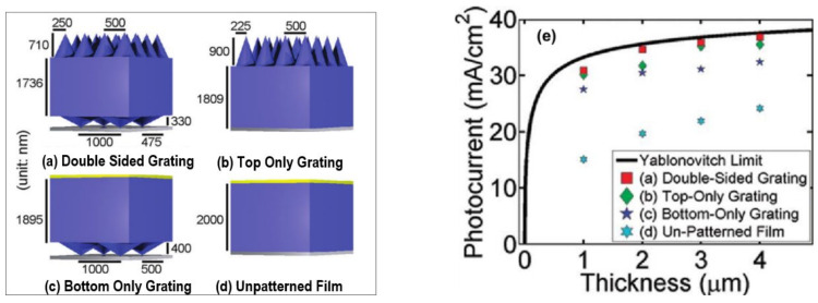
Figure 13.
Three-dimensional silicon thin-film structures in air. From (a) to (d), blue represents silicon, gray represents a perfect electric conductor (PEC), and yellow represents nonabsorbing silicon nitride. The nanocones were made of silicon, as were the uniform layers, and they were placed in a two-dimensional square lattice either on the front or on the back surface of the film. (a) The optimized double-sided nanostructure. (b) The optimized top-only nanostructure. (c) The optimized bottom-only nanostructure with a thin layer of nonabsorbing silicon nitride on top. (d) The flat film with a thin layer of nonabsorbing silicon nitride on top [178]. (e) Photocurrents generated by structures as a function of their equivalent thicknesses. (Reprinted with permission from [178], 2012, American Chemical Society).

