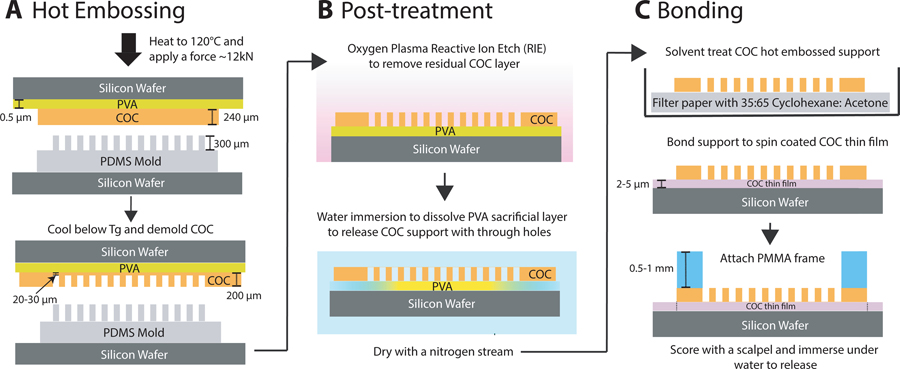
Figure 2:
A schematic of the fabrication scheme used to produce the top and bottom sides of the microfluidic chip (as shown in Figure 1). (A) Hot embossing was performed using an elastic PDMS mold to imprint an array of “X-ray window” features in COC sheets (240 μm). (B) The residual thin film (20–30 μm) from the embossing step was removed using oxygen plasma reactive ion etching (RIE) to create COC supports (~200 μm) with through-hole windows. The supports were detached from the silicon wafer by dissolving the PVA sacrificial layer in water. (C) To assemble each side (top and bottom), a COC support was solvent treated to facilitate bonding to COC thin films of desired thicknesses (2–5 μm), followed by attachment of a 0.5–1 mm thick PMMA frame using an adhesive layer to provide rigidity and flatness.

