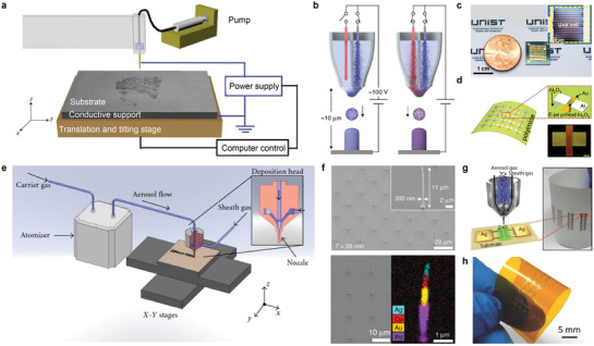
Figure 5.

Inkjet‐based 3D printings. a) Schematic illustration of the electrohydrodynamic jet printer setup. b) Schematic illustration of the electrohydrodynamic redox printing multichannel nozzle. c) Photograph of the UHD SS‐MSCs fabricated on a chip (area = 8.0 mm × 8.2 mm, smaller than a coin). Inset shows an optical microscopy image of the unit cell in the UHD SS–MSCs. d) Schematic illustration of the e‐jet‐printed flexible In2O3 TFT array on a PI substrate and optical micrograph of a single transistor on th.e PI substrate. Scale bar, 50 µm. e) Schematic illustration of the aerosol jet printing system. f) SEM image (bottom left) and EDS map (bottom right) of nanopillars consisting of Pd (purple), Au (yellow), Cu (red) and Ag (light blue). g) Schematic illustration of aerosol jet deposition head demonstrating the aerodynamic focusing of aerosol gas stream on the device architecture of the printed photodetector on PET substrate and optical image of fully aerosol‐jet printed array of ZnO photodiodes on a mechanically flexible PET substrate. h) Photograph of flexible CNT‐TFTs and logic circuits on a Kapton film. a) Reproduced with permission.[ 93 ] Copyright 2007, Nature Publishing Group. b) Reproduced with permission.[ 99 ] Copyright 2019, Springer Nature. c) Reproduced with permission.[ 100 ] Copyright 2020, American Association for the Advancement of Science. d) Reproduced with permission.[ 63 ] Copyright 2016, The Royal Society of Chemistry. e) Reproduced under the Creative Commons Attribution License.[ 101 ] Copyright 2021, Beilstein. f) Reproduced with permission.[ 95 ] Copyright 2021, Springer Nature. g) Reproduced with permission.[ 106 ] Copyright 2018, American Chemical Society. h) Reproduced with permission.[ 107 ] Copyright 2017, Wiley‐VCH.
