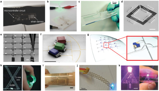
Figure 8.

3D‐printed interconnects. a) Image of textile‐mounted printed strain sensor and microcontroller unit. b) Photograph of 3D Cu circuit formed by 3D printing and 3DLW process. c) Four printed and sintered silver pillars using silver nanoparticle ink. d) SEM image of 20 electrodeposited interconnects. Scale bar, 10 µm. e) Optical image of patterning of silver interconnects on a gallium arsenide‐based, 4‐by‐4 LED chip array. f) Colorized SEM image of three LED pixels and EGaIn interconnects. Scale bar, 1 mm. g) Schematic illustration of the microLED array with reconfigured 3D interconnects. h) Photographs of e‐jet printed two‐layer circuit that connected a battery to light a LED. i) Photograph of circuits in a flexible substrate (PET) with the GO/MWCNT hybrid ink. Scale bar, 1 cm. j) Photograph of a two‐terminal LED powered through a dual‐path FSCW. k) Photograph of a e‐jet printed conductor on PDMS with Christmas tree pattern that connected a battery to light a LED. Scale bar, 500 µm. a) Reproduced with permission.[ 81 ] Copyright 2017, Wiley‐VCH. b) Reproduced with permission.[ 144 ] Copyright 2020, Wiley‐VCH. c) Reproduced with permission.[ 145 ] Copyright 2019, Wiley‐VCH. d) Reproduced with permission.[ 8 ] Copyright 2010, The American Association for the Advancement of Science. e) Reproduced with permission.[ 146 ] Copyright 2009, The American Association for the Advancement of Science. f,g) Reproduced with permission.[ 9 ] Copyright 2021, American Association for the Advancement of Science. h) Reproduced with permission.[ 147 ] Copyright 2021, Wiley‐VCH. i) Reproduced with permission.[ 148 ] Copyright 2018, American Chemical Society. j) Reproduced with permission.[ 149 ] Copyright 2019, Wiley‐VCH. k) Reproduced with permission.[ 150 ] Copyright 2017, Wiley‐VCH.
