Figure 4.

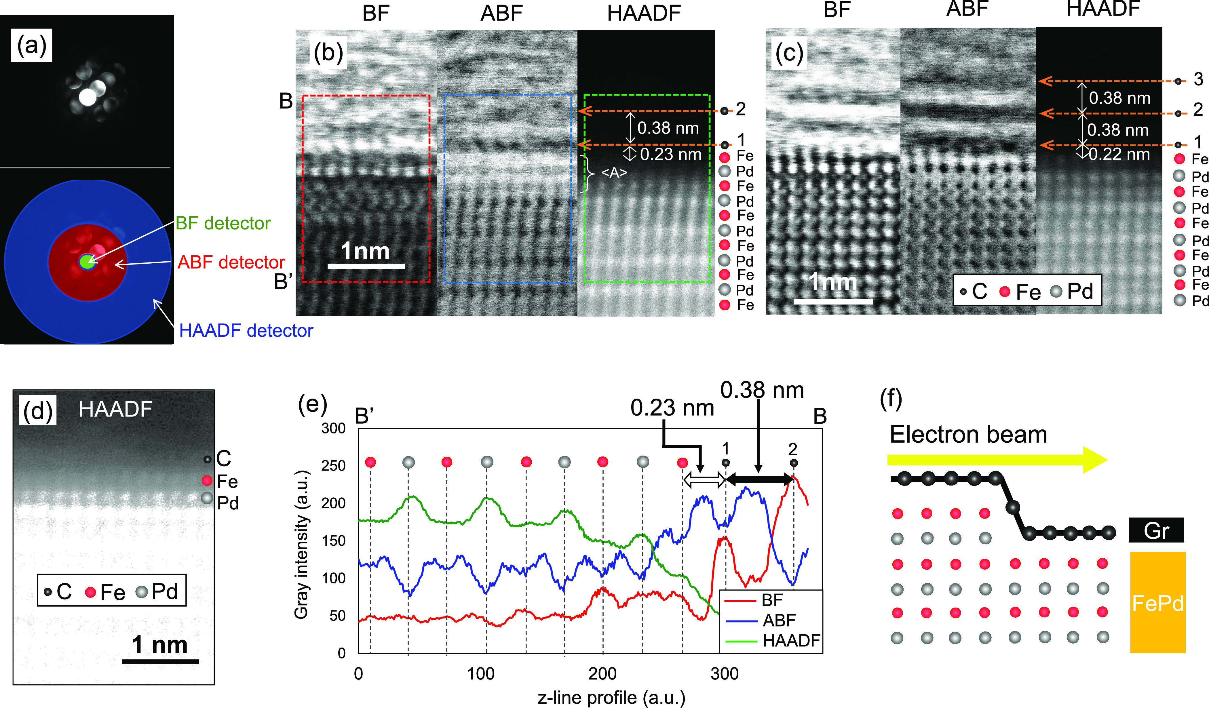
Cross-sectional scanning tunnel electron microscopy (STEM) observations using three different detectors: bright-field (BF), annular bright-field (ABF), and high-angle annular dark-field (HAADF). The incidence of the electron beam is [110]L10. (a) Acceptance angles for BF, ABF, and HAADF were 0–10.1, 10.1–79.5, and 79.5–200 mrad, respectively. STEM observation for (b) single or bilayer graphene and (c) trilayer graphene. (d) Visualization of the interface of the FePd-side HAADF-STEM image by contrast adjustment. The outermost surface atom of FePd was identified primarily as Fe rather than Pd. (e) z-line profiles of the out-of-plane direction obtained from STEM images in (b). z-line profile averaged from the x-direction in the dashed square area. (f) Schematic illustration of electron beam incident direction to the step–terrace interface formed at the Gr/FePd layer.
