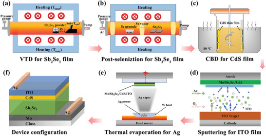
Figure 1.

Schematic illustration of the preparation process of the substrate structured Sb2Se3 thin‐film solar cell. a) VTD process for Sb2Se3 thin film. b) Post‐selenization heat treatment of Sb2Se3. c) CdS buffer layer deposited via chemical bath deposition (CBD) method. d) ITO layer deposited by magnetron sputtering. e) Ag electrode prepared via thermal evaporation process. f) Schematic configuration of the final Sb2Se3 device.
