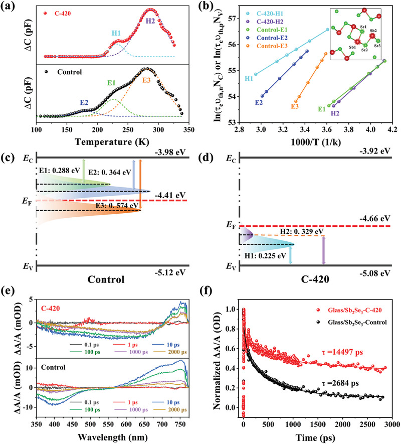
Figure 7.

a) DLTS signals from the Control and C‐420 Sb2Se3 devices, b) The corresponding Arrhenius plots obtained from DLTS signals. c,d) Conduction (E C) and valence (E V) band edges, Fermi level (E F) and defect energy levels of the Control and C‐420 samples, respectively. e) Time‐resolved absorption spectra obtained at various time delays after photoexcitation for the Control and C‐420 Sb2Se3 thin films. f) Transient kinetic traces showing the decay of the PIA peak at 750 nm for both thin films.
