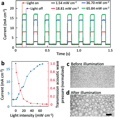
Figure 2.

a) The electrical current through the silicon wafer under a certain voltage indicates the reversible alternative change between low conductivity state (no illumination) and high conductivity state (illumination). b) As the light intensity projected on the wafer surface increases, the photocurrent increases, and the transmission acoustic pressure decreases due to the boost of the microbubble generation. Microscopic images of c) the silicon wafer surface before illumination and d) the generated microbubbles on the silicon wafer surface after illumination. The light intensity was 65 mW cm–2 and the projection time was 0.1 s. The scale bar is 0.2 mm.
