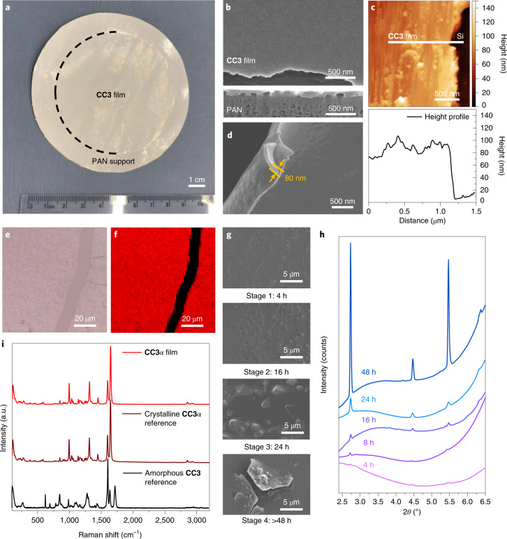
Fig. 2. Characterization of a CC3α film.
a, Photograph of composite membrane CC3α-PAN with a diameter of 7.4 cm. b, SEM image of CC3α-PAN showing the surface morphology of the CC3α film. Shown below is the cross-sectional FIB-SEM image of CC3α-PAN. c, AFM height image (top) and the height profile (bottom) of CC3α film transferred onto a silicon (Si) wafer. d, SEM image of a free-standing CC3α film, where the film was deliberately buckled to show its thickness. e,f, Raman microscope image (e) and Raman map (f) of a CC3α film on a glass support, where we purposely scratched the film before the measurement to expose the glass support (black stripe in f). The red regions on a CC3α film had comparable Raman spectra to the crystalline CC3α reference sample. g, SEM images of CC3α-PAN-X h-0.8% membranes formed at different reaction times, showing four stages of CC3α film formation. h, Out-of-plane GIXRD (wavelength, λ = 0.689 Å) patterns of CC3α-PAN-X h-0.8% membranes fabricated using reaction times between 4 and 48 hours (2θ refers to the scattering angle). i, Raman spectra of CC3α film, a crystalline CC3α reference1 and an amorphous CC3 reference3.

