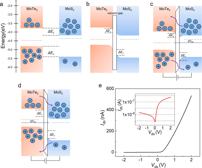
Figure 2.
Energy band diagrams and electrical figures of the MoTe2–MoS2 device. (a) Band diagrams before contact. (b) Band diagrams after contact. (c) Carrier transport band diagrams under forward bias. (d) Carrier transport band diagrams under reverse bias. (e) I–V curves of the MoTe2–MoS2 device; the inset picture represents the I–V characteristics in the logarithmic coordinate. The characterization of this device can be found in Figure S2 in the Supporting Infromation.

