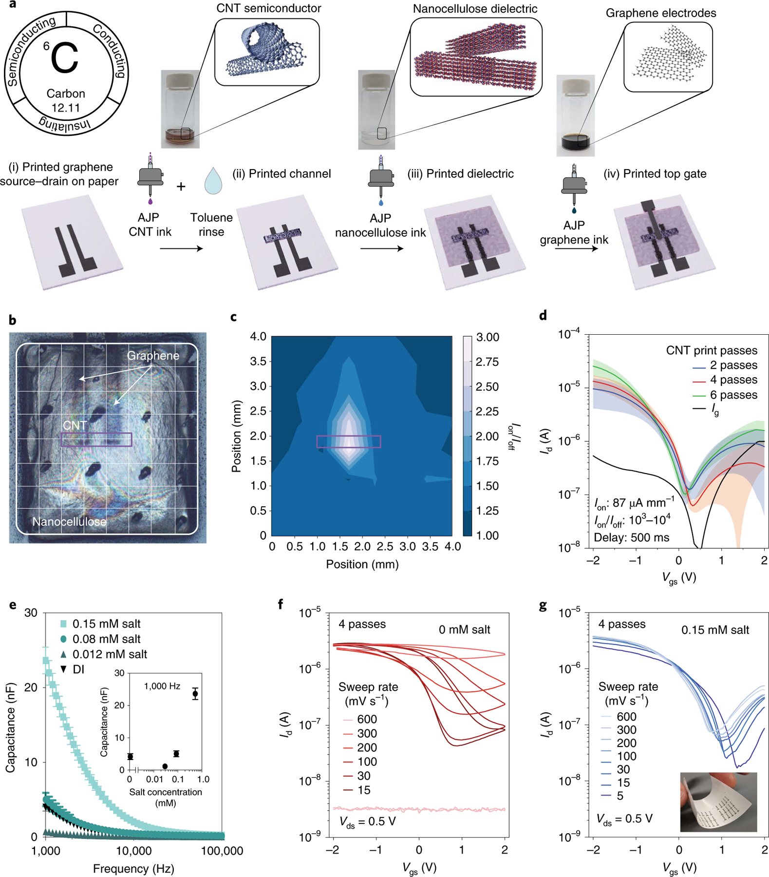
Fig. 2 |. All-carbon TFT printing and testing.

a, printing fabrication schematic with all-carbon inks. AJp, aerosol jet printing. b, Top-view optical image of the all-carbon TFT without a printed top gate. c, Surface map of transistor Ion/Ioff as a function of gating location (determined by probe placement on the nanocellulose thin film) for the TFT in b. d, Subthreshold curves as a function of CNT print passes. The data represent the average value (line) ± standard deviation (shaded region) of 12 devices without added salt at a Vds of −0.5 V. e, Frequency-dependent capacitance versus ink salt concentration (with values at 1,000 Hz shown in the inset). f,g, Subthreshold curves measured with different sweep rates for devices with no added salt (f) and with 0.15 mM NaCl added (g) to the nanocellulose ink, which yields robust switching even with a 600 mV s−1 sweep rate. The inset in g is a photograph of an array of all-carbon transistors. All devices in this report have a channel length of 250 μm and a channel width of 200 μm.
