
Fig. 4 |. All-carbon TFTs with demonstration of controlled recycling.
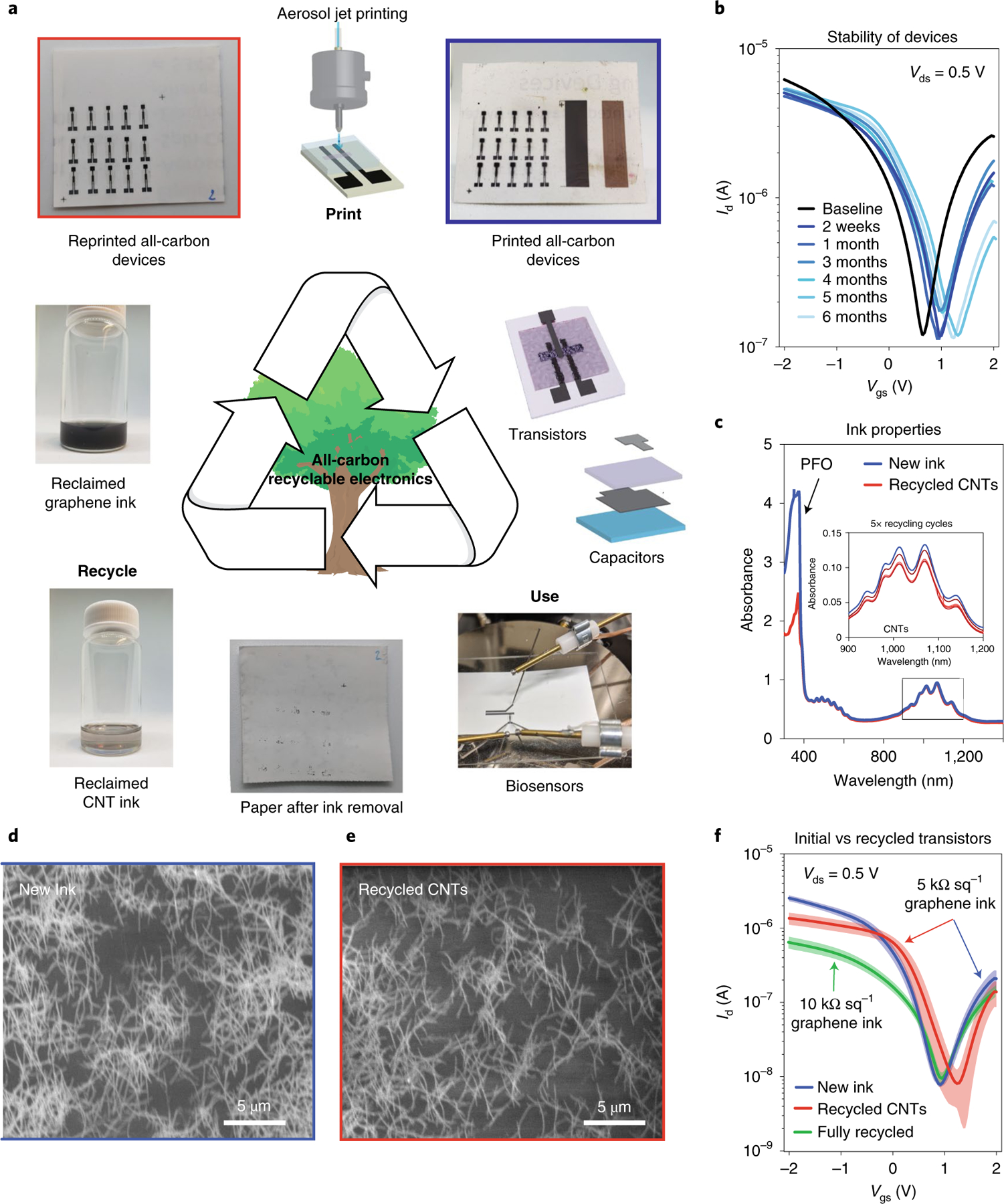
a, Schematic of the all-carbon recyclable electronics system, demonstrating printing, use (see Extended Data Fig. 8 for a biosensing demonstration) and recycling, then reprinting, reuse and so on. The top right inset shows an array of all-carbon recyclable electronic TFTs with excess graphene (left) and CNTs (right) printed to the side. b, Stable TFT characteristics over six months of storage in air. The transistor was fabricated without salt and run with a sweep rate of ~30 mV s−1. c, UV–vis–Nir spectra of new ink and five iterations of CNT ink recycling, showing minimal loss in ink concentration over the five recycling cycles. d,e, SEM images of printed new (d) and recycled (e) CNT inks. f, Subthreshold curves of transistors from new and recycled inks, with nominally consistent performance using recycled CNTs and slight reduction with recycled CNTs and graphene due to the increased graphene sheet resistance (attributed to increased bundling in the recycled ink). The data represent average ± standard deviation of four devices with a salt concentration of 0.15 mM in the nanocellulose and a sweep rate of ~600 mV s−1.