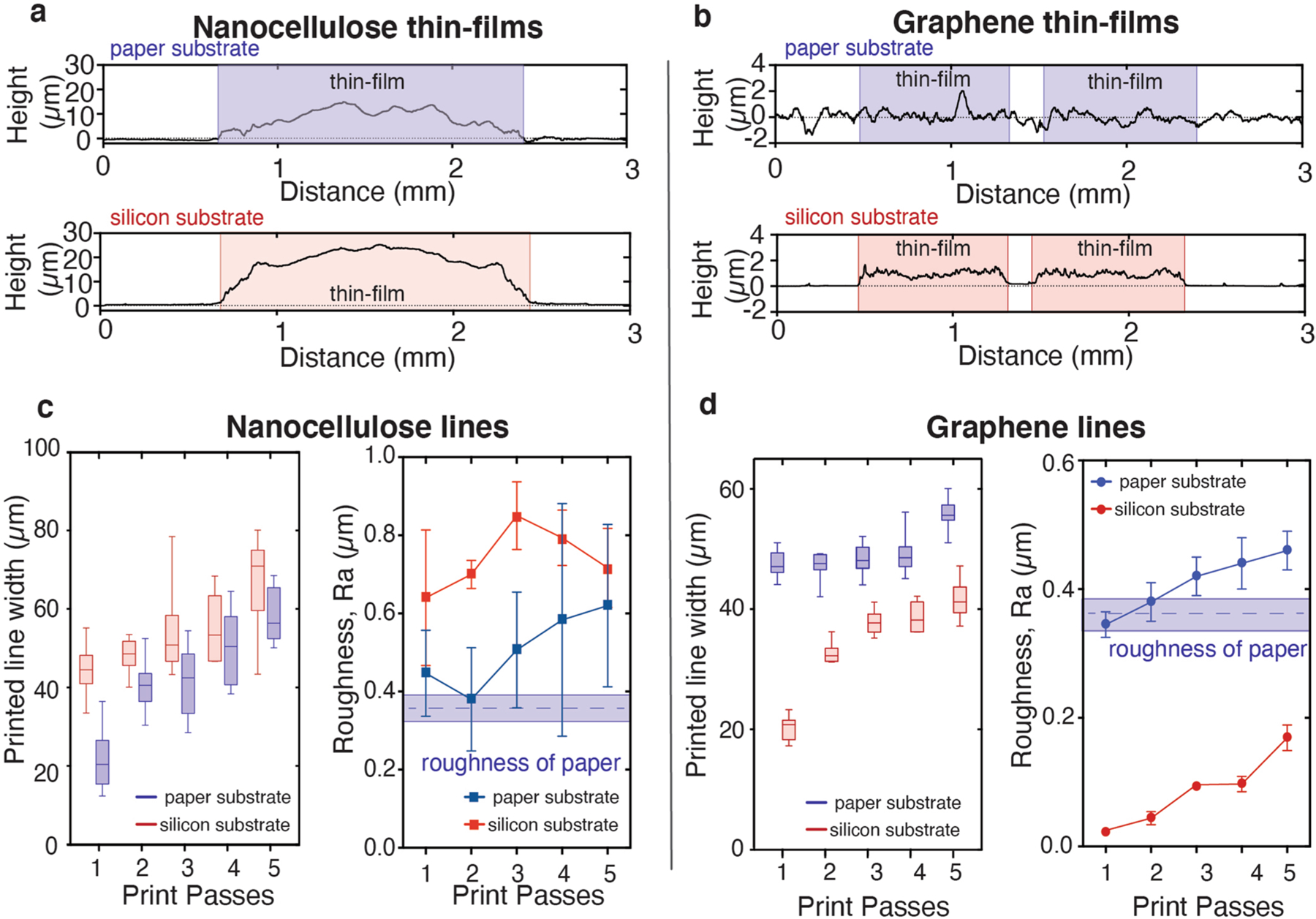
Extended Data Fig. 2 |. Characterization of printed inks.

a, Heights of single pass nanocellulose thin-films printed onto a paper substrate (top) and silicon substrate (bottom). Boxed region represents printed thin-film area. The height of the CNC thin-film is most likely lower on the paper substrate due to impregnation of the nanocellulose film into the fibrous paper. b, Heights of graphene thin-films printed onto a paper substrate (top) and silicon substrate (bottom). Boxed region represents printed thin-film area. No graphene height can be observed on the paper substrate due to wicking of the ink into the paper substrate. c, printed line widths (left) for nanocellulose lines printed onto paper substrates (blue) and silicon substrates (red) as a function of print passes. Box represents lower and upper quartile range, line represents median, and whiskers represent lowest and highest value. Line widths represent 10 width measurements from 1 print. printed line roughness values (right) for nanocellulose lines. Datapoints represent average and standard deviation of 5 profilometry measurements taken from 1 print. d, Graphene line widths (left) and roughness values (right) for printed lines on paper substrates (blue) and silicon substrates (red).
