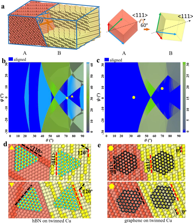
Fig. 1. 2D materials alignment on twinned Cu substrates.
a Atomic configuration of a 60° <1 1 1> twin in a Cu foil and the definition of the two degrees of freedom, (θ, ψ), of the twin structure. Where θ is the angle between the Cu foil surface and the twin boundary and ψ is the in-plan rotation angle of the twin plane. The crystal axials of the two crystal lattices on both sides of the twin boundary (A and B) and their <1 1 1> co-axis is also shown. b Theoretical map of the misalignment angles between 3-fold symmetric 2D materials grown on the two sides of FCC twins as a function of (θ, ψ), which define the facet indices of the twinned surface. Colour bar shows the misaligned angles between 2D materials grown on twinned crystal surfaces and blue indicates perfect alignments. c Theoretical map of the misalignment angles between 6-fold symmetric 2D materials, such as graphene, grown on both sides of FCC twins as a function of (θ, ψ). Colour bar shows the misaligned angles of 2D islands grown on the twinned crystals and blue denotes perfect alignment. We can clearly see that the unidirectional alignment of 2D materials with either 3-fold or 6-fold symmetry can be realized on a large number of twinned FCC crystals. So, in principle, this should allow us to use a variety of twinned substrates to grow 2D single crystals. d Schematic diagram of hBN epitaxy on twinned Cu substrates, Cu atoms of step edges are highlighted. The alignment directions of hBN islands are denoted by dashed lines. e Schematic diagram of graphene epitaxy on twinned Cu substrates, Cu atoms of step edges are highlighted. The alignment directions of graphene islands are denoted by dashed lines.

