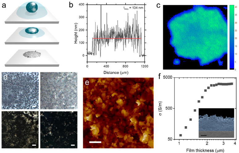
Figure 2.
(a) Schematic illustration of emulsion droplet deposition, drying and collapse. (b) Stylus profilometry of deposited droplet showing film thickness of ∼130 nm, corresponding to ∼30 monolayers interfacial film thickness. (c) Raman map of G peak intensity illustrating the uniformity of deposited film; 30 × 30 μm image. (d) Low-magnification optical micrographs of deposited droplets on PET showing the sequential passes of emulsion deposition with percolation and formation of densely packed films; scale bars 500 μm. (e) Atomic force micrograph of nanosheet film confirming dense and uniform areal packing of the nanosheets deposited from a single emulsion droplet; scale bar 500 nm, height range 200 nm. (f) Electrical conductivity of the graphene film deposited from emulsion as a function of film thickness showing the scaling attributed to deposition uniformity, which reaches expected bulk-like value. Inset: Scanning electron micrograph of film cross section (false colored) showing the dense-packed nanosheet network; scale bar 1 μm.

