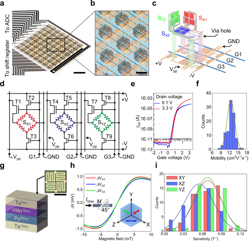
Fig. 2. Structure and magnetoelectrical performance of the IMOS device.
a Photo of an IMOS device with 8 × 8 pixel matrix. Scale bar, 2 mm. b Image of the pixel array in the device. The pixel pitch is 1.1 mm × 1.1 mm. Scale bar, 500 µm. c, d Exploded schematic and circuit diagram of a single pixel which contains three subpixels. The Wheatstone bridge type AMR sensors on the three orthogonal planes are marked as SXY, SXZ and SYZ respectively. e Typical transfer characteristics with VGS from -2 V to 3.3 V for the a-IGZO TFTs. The leakage currents are plotted in gray lines. f Statistics of the mobility µ. Histogram of µ for 100 a-IGZO TFTs. The average µ is (12.51 ± 1.32) cm2 V−1 s−1. g Schematic illustration of the layer stack of the AMR sensors. Inset is a micrograph of the AMR sensor. Scale bar indicates 200 µm. h Typical responses of the SXY, SXZ and SYZ sensors. The left inset shows the 45° angle between the bias current and the magnetization direction. The right inset shows the orientations of the sensitivity directions of SXY, SXZ, and SYZ. For all the tests Vpp = VG = 3.3 V. i Histograms of the sensitivities for the working sensors on the XY, XZ, YZ planes in a typical 8 × 8 sensor array. The sensitivities are normalized to Vpp of 3.3 V. Source data are provided as a Source Data file.

