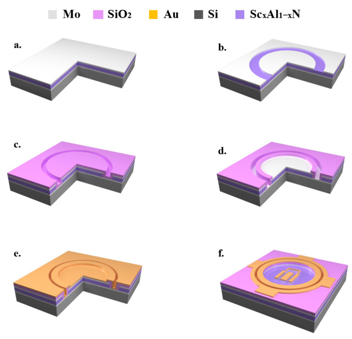
Figure 1.
The process flow of the PCM structure. (a) a stack of Mo/AlN(AlScN)/Mo is deposited by magnetron sputtering; (b) a 0.2 µm Mo top layer is patterned and etched as a hard mask for the underlying AlN/AlScN layer etching; (c) a 1 µm layer of SiO2 is deposited by PECVD; (d) the top and bottom electrodes are exposed after SiO2 patterning; (e) a 0.5 µm layer of Ti/Au was deposited; (f) the top Au electrode was patterned for electrical connection.

