
Fig. 3 |. Typical inorganic semiconductors used for EGTs.
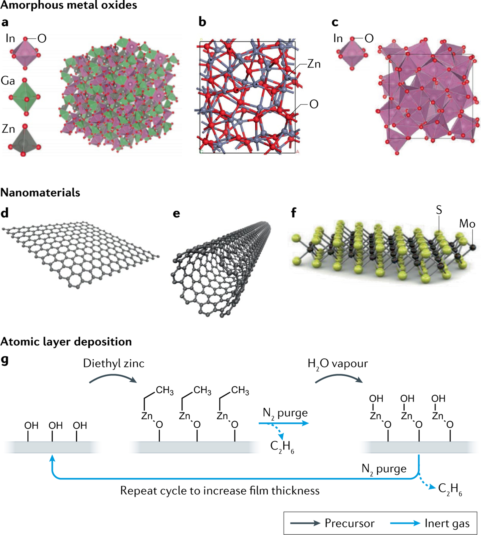
a | Amorphous structure of indium–gallium–zinc oxide (IGZO). b | Structure of amorphous zinc oxide (ZnO). c | Structure of amorphous indium oxide (InO3). d | Two-dimensional layer of the semimetal graphene. e | Single-walled carbon nanotubes. f | Two-dimensional molybdenum disulfide (MoS2). g | Atomic layer deposition is one method to deposit thin films of inorganic semiconductors on a substrate. Precursors injected into the chamber react with the surface of the substrate, building the film up layer by layer. Purge steps in between with inert gas remove by-products and undesired precursor from the chamber. Atomic layer deposition ultimately enables control over film thickness and uniformity. EGT, electrolyte-gated transistor. Part a adapted with permission from REF.312, ACS. Part b adapted from REF.313, CC BY 4.0 (https://creativecommons.org/licenses/by/4.0/). Part c adapted with permission from REF.314, Wiley. Parts d and e adapted from REF.315, CC BY 4.0 (https://creativecommons.org/licenses/by/4.0/). Part f adapted with permission from REF.316, Elsevier.