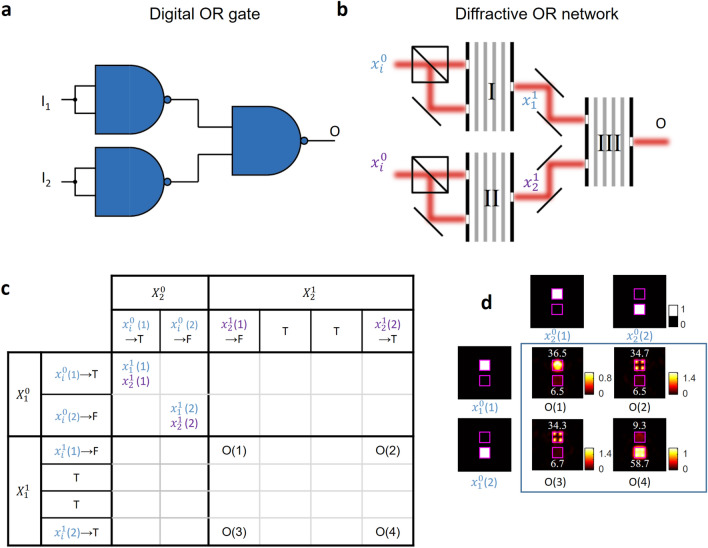
Figure 4.
Logical OR operator that is composed of cascaded diffractive NAND gates. (a) Digital implementation of an OR operator using NAND gates. (b) All-optical OR gate that is composed of cascaded diffractive NAND gates. (c) A portion of the design map (Fig. 2b) showing the correctness of the intermediate all-optical calculation steps () and the output of the OR gate (O) under different input combinations. (d) The intensity profiles at the output plane of the final diffractive NAND gate. The inserted numbers in white font color indicate the relative optical signal within each aperture. Each input optical logical value is assumed to have a relative optical signal level of 256 (a.u.), defining the ideal signal level per aperture.

