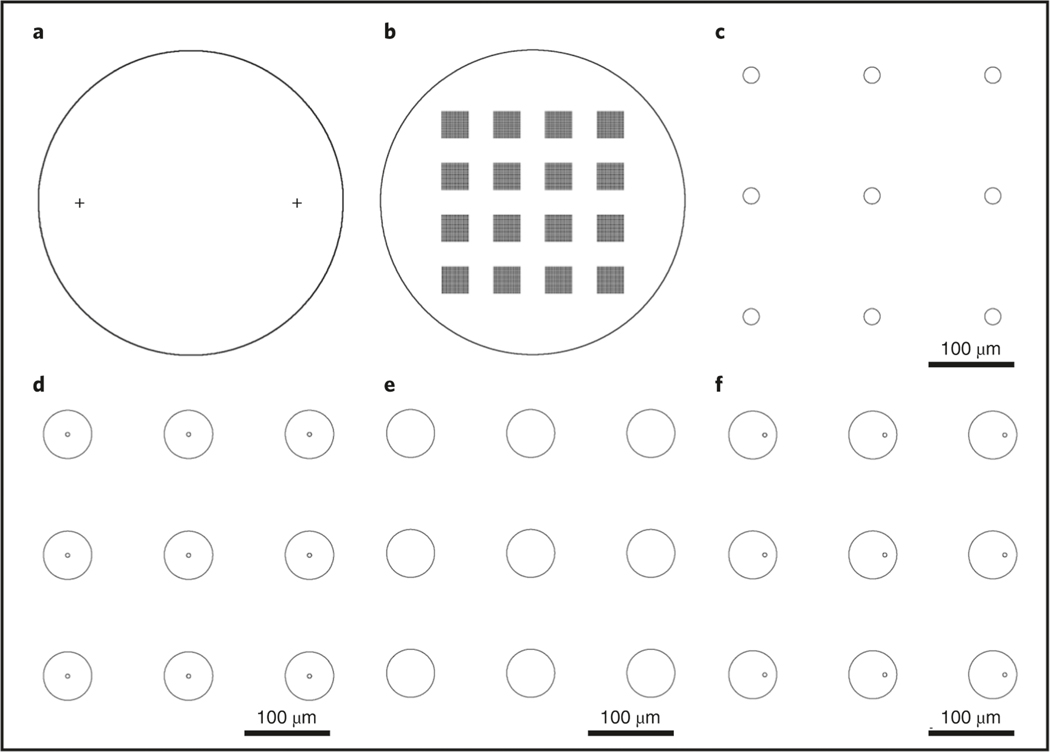
Fig. 3 |. Typical lithography patterns for needle arrays in the fabrication process.
a, Two alignment marks, each having a width of 20 μm, are symmetrically located on a 4-inch Si wafer, both 35 mm away from the center point. b, 4 by 4 chips are arranged on a 4-inch Si wafer with a 17-mm period. Each chip has a 60 by 60 array of the needles with a 150-μm period (distance between the needles on the chip). c, The backside etching mask of holes with the size of 20 μm, with a 150-μm period. d, The layout of the primary Type I needle array with a 55-μm diameter and a 150-μm period; the center bore size is 5 μm. e, The layout array with a 55-μm diameter and a 150-μm period used to generate the SiO2 protection layer in the isotropic etching step of the Type II needle. The layout in d is reused in the fabrication process of the Type II needle array. f, The layout of the Type III needle array with 55-μm diameter and 150-μm period; the 5-μm bore is positioned 15 μm from the center. The layout in e is reused in the fabrication process of the Type III needle array.

