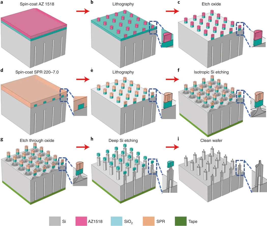
Fig. 7 |. Schematics of the fabrication process for the hollow needles with sharp tip and centered bore (Type II).
a, Spin-coat AZ 1518 photoresist on the front side with PECVD SiO2 coating (Step 1B(iii–v)). b, Expose the layout (Fig. 3e) using the maskless aligner followed by development (Step 1B (vi–vii)). c, Etch away the SiO2 layer without the photoresist covering using DRIE (Step 1B(viii)). D, Remove the residual AZ 1518 and spin-coat SPR 220-7.0 photoresist (Step 1B(ix–xiii)). E, Pattern the donut-shaped arrays (Fig. 3d) (Step 1B(xiv–xvi)). F, Cover the backside holes using polyimide tape and carry out isotropic Si etching to obtain sharp tips (Step 1B(xvii–xviii)). g, Etch through the SiO2 layer in the center to expose the Si underneath (Step 1B(xix)). h, Form the hollow-needle array with the deep Si etcher (Step 1A(xxiii)). i, Remove the residual photoresist and oxide, followed by cleaning the wafer (Step 1A(xxiv–xxix)).

