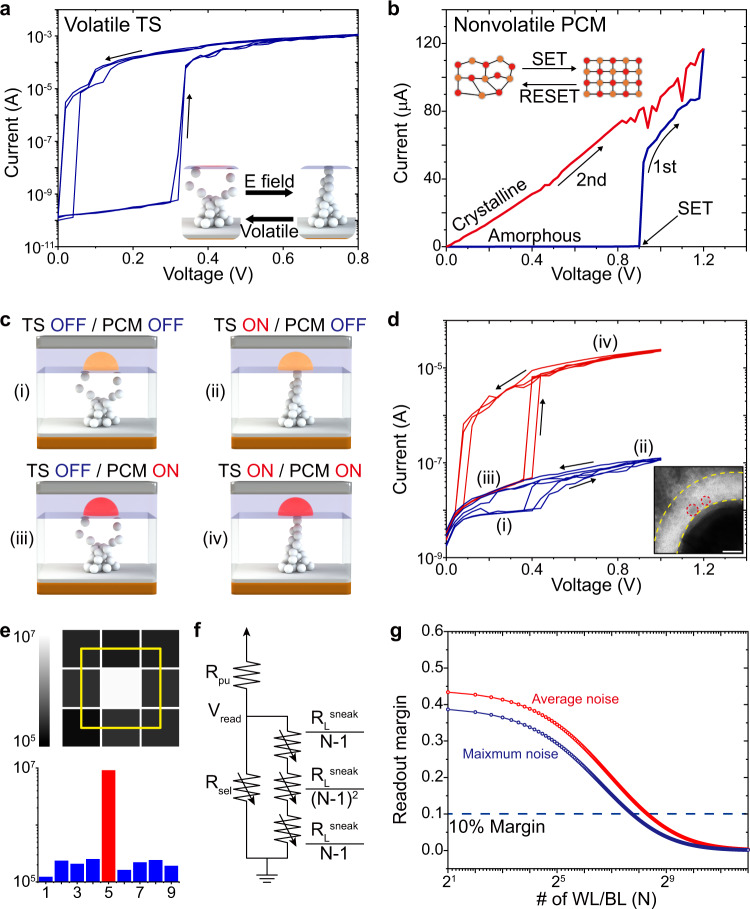
Fig. 2. Electrical characteristics of volatile TS, nonvolatile PCM, and unified TS-PCM.
a Current-voltage (I-V) curve of volatile TS device presenting threshold switching at 0.33 V and spontaneous reset. b I-V curve of PCM showing nonvolatile resistive switching by voltage sweep (blue). The second sweep (red) exhibits a high current value, indicating the nonvolatile phase transition of the GST film. c Schematic diagram of four stages in TS-PCM operation. Both TS and PCM layers are in the OFF state in stage (i) with high resistance. The TS layer is switched to the ON state in stage (ii) with relatively low resistance. The top PCM layer is switched to the ON state by Joule heating of the Ag filament in stage (iii), which shows high resistance due to the bottom TS layer. Both the TS and PCM layers are in the ON state in stage (iv), which shows the lowest resistance. d I-V curve of TS-PCM presenting the four stages illustrated in c. Inset shows a TEM image of the TS-PCM cell with Ag clusters in the SiO2 matrix. Scale bar, 10 nm. e Resistance-based color map (upper panel) and bar graph (lower panel) of worst-case scenario that verifies the random-access capability of TS-PCM. f Illustration of circuit model utilized in the OBPU method. For a sufficiently large N, RLsneak/(N-1)2 becomes negligible. g Calculated readout margin by OBPU method. The TS-PCM array can be scaled up to 316 × 316 for a 10% readout margin in average noise case (red curve). The maximum array size of TS-PCM is decreased to 214 × 214 in maximum noise case (blue curve).

