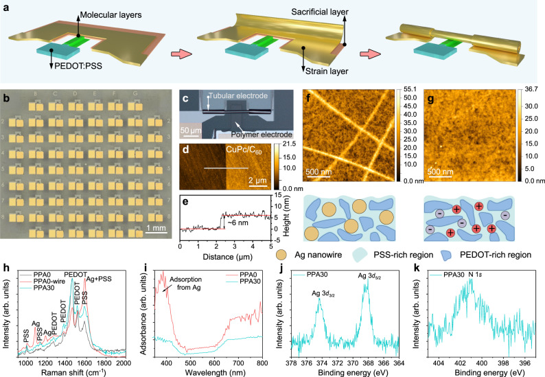
Fig. 2. Design and microfabrication of the molecular devices.
a Formation of rolled-up soft contacts. The finger-shaped mesa structure provides a platform for the bottom electrode, onto which molecular layers are grown. During the selective etching of the sacrificial layer GeOx by deionized (DI) water, the Au/Ti/Cr nanomembranes release their built-in stress and roll up. After rolling, the rolled-up metallic nanomembrane bonds as a top electrode to the molecule layer below, forming a sandwich structure. b Micrograph of the molecular device array. c–e Typical single device based on a rolled-up soft contact (c). The width of the bottom electrode and the diameter of the rolled-up metallic tube are ~40 μm and ~10 μm, respectively. AFM image of CuPc (3 nm)/CuPc (3 nm) grown on the wafer (d) and the corresponding height profile (e). f, g AFM images of the spin-coated PEDOT:PSS:AgNWs film before (f) and after (g) 30 s wet etching. Schematic illustrations are also given. h, i Raman spectrum (h) and adsorption coefficient profile (i) of the spin-coated PEDOT:PSS:AgNWs film before (denoted as PPA0) and after 30 s wet-etching (denoted as PPA30). j, k XPS spectra (Al-Kα = 1486.6 eV) corresponding to Ag 3d (j) and N 1 s (k) of the etched PEDOT:PSS:AgNWs film.

