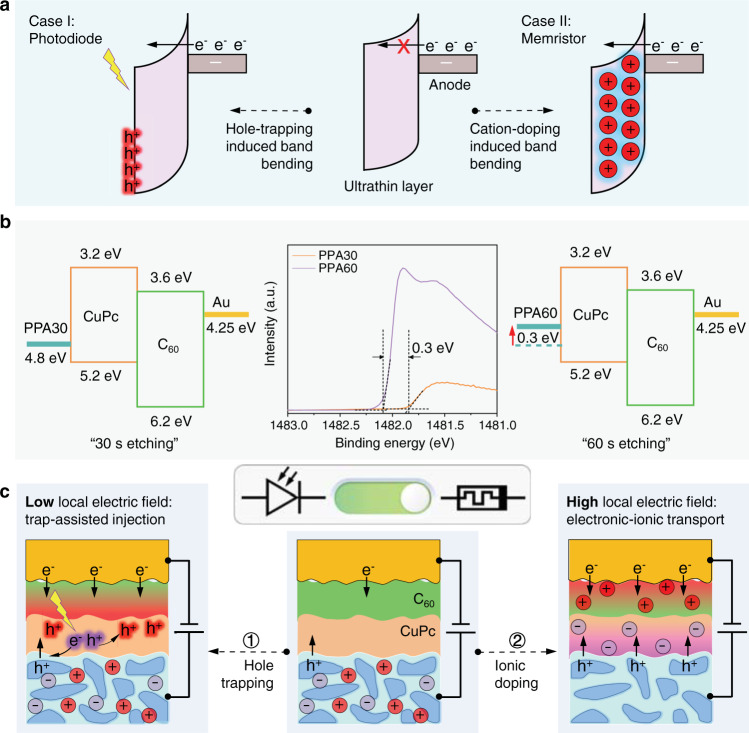
Fig. 5. Mechanism of the electric-field-driven transition.
a Both trapped holes and accumulated ions in the vicinity of the electrodes have the same effect, i.e., they induce band bending and enhance the charge injection due to the increase in the local carrier density. Red-glowing “h+”, red circle with “+”, and black “e−” represent the trapped photogenerated hole, accumulated cation, and injection electron, respectively. b Photoelectron spectra (Al Kα-monochromated, 300 W, 1486.6 eV) of the wet-etched PEDPT:PSS:AgNWs and the proposed band structures (before equilibrium) with 30 s-etching and 60 s-etching. From the photoelectron spectra obtained by using monochromatic Al Kα radiation, the calculated values of the work function for PPA30 and PPA60 are 4.8 eV and 4.5 eV, respectively. c At a low local electric field across the PPA/CuPc interface, electronic transport dominates, resulting in photomultiplication photodiodes as demonstrated in Fig. 3. At a high local electric field across the PPA/CuPc interface, ion migration is activated, resulting in bipolar memristors as demonstrated in Fig. 4. Therefore, by controlling the PPA/CuPc interface electric field, the molecular device can be switched between the photomultiplication photodiode and bipolar memristor.

