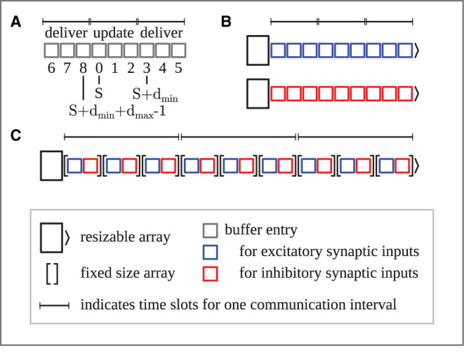
Figure 8.

Neuronal input buffers accounting for synaptic delays in simulations of spiking neuronal networks. (A) Structure of neuronal input buffers assuming a minimum synaptic delay dmin of three simulation time steps and a maximum delay dmax = 2dmin. To buffer upcoming inputs during simulation a total buffer size of dmin+dmax time slots is required, which corresponds to three communication intervals of three simulation time steps each. After every spike communication and subsequent spike delivery to local targets, simulation time is advanced, meaning that the relative time origin S of the neuronal input buffers advances by dmin time slots with a wrap-around at the buffer end. A pre-calculated and continuously updated look-up table maps the index relative to S to the actual buffer index. Example: The relative time origin S is located at the fourth time slot. Synaptic delays of the inputs of the middle buffer segment elapse with the upcoming three simulation time steps; the neuron integrates these inputs updating its state. Spikes are then communicated and new inputs delivered to the neuron are added to the time slots in the last or first buffer segment depending on the delay, which is at least dmin and at most dmax. Relative time origin S then advances to the seventh buffer slot (not shown). (B) Original neuronal spike buffers for two input channels (e.g., excitatory and inhibitory synaptic inputs). For each channel a separate resizable array buffers the inputs for the upcoming time slots. (C) Multi-channel input buffer for two input channels. A single resizable array stores the inputs for the upcoming time slots, where for each time slot a fixed size array holds the inputs sorted by channel.
