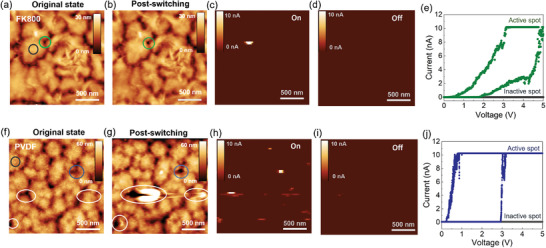
Figure 2.

Comparing the morphological integrity of FK‐800 and PVDF‐based memristors before and after switching via conductive AFM. Topography image of the FK‐800 a) before applying a voltage and b) after cycling. c) Corresponding current map in the on‐state using a bias of 5 V and a compliance current of 10 nA. d) Corresponding current map in the off‐state using a bias of 0.2 V. e) I–V sweep at the active spot indicated in the green circle in (a) and inactive spot indicated by the grey circle in (a). There are no obvious changes in morphology due to switching. To compare, a PVDF device was scanned under the same conditions. Topography image of the PVDF film f) before applying a voltage and g) after cycling. h) Corresponding current map in the on‐state using a bias of 5 V and a compliance current of 10 nA. i) Corresponding current map in the off‐state using a bias of 0.2 V. j) I–V sweep at the active spot indicated in the blue circle in (f) and inactive spot indicated in the gray circle in (f). White circles in (f) and (g) highlight active spots where there is evidence of irreversible morphological changes due to switching. All images are 2 µm × 2 µm. The vertical scale is provided as an inset.
