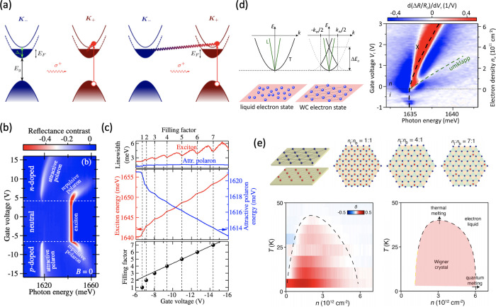
Figure 11.
(a) Schematic band structure depicting intravalley (left) and intervalley (right) interactions between an exciton and a spin-polarized 2DES in a lightly doped W-based ML TMD. Adapted with permission from ref (170). Copyright 2020 AIP Publishing. (b) Voltage-gate-dependent color-scale map presenting reflectance contrast spectra measured in an hBN-encapsulated ML MoSe2. Attractive and repulsive exciton polarons are visible in both n- and p-doped regimes. Adapted with permission under a Creative Commons CC BY 4.0 license from ref (171). Copyright 2019 American Physical Society. (c) Gate-voltage dependencies of the line widths (top panel) and energies (middle panel) of the exciton (red) and attractive polaron (blue) resonances on the hole-doped side of an hBN-encapusulated ML MoSe2 at B = 16 T. Bottom panel: Gate voltages corresponding to integer filling factors determined based on the positions of the local minima of the exciton line width. Adapted with permission under a Creative Commons CC BY 4.0 license from ref (171). Copyright 2019 American Physical Society. (d) Gate-voltage-dependence derivative of the reflectance contrast spectrum with respect to the gate voltage of a charge-tunable, dual-graphene-gated, and fully hBN-encapsulated MoSe2 ML (right panel). The weak, higher-energy resonance is due to Umklapp scattering of the excitons off the electron Wigner crystal. Left panel: Schematics of the exciton dispersion in a ML TMD semiconductor hosting an electron system in various structural phases. The parabolic- and linear-in-momentum exciton branches arise from the splitting of the exciton branches due to the electron–hole exchange interaction, and correspond to the exciton dipole oriented along transverse (T) or longitudinal (L) directions with respect to the momentum vector, respectively. Adapted with permission from ref (172). Copyright 2021 Springer Nature. (e) Top panels: schematics of a Wigner crystal in a MoSe2 bilayer with an intercalated 1 nm thick layer of hBN (left). The top right panels show schematics of commensurate stacking in bilayer Wigner crystals with triangular lattices for filling ratios nt:nb of 1:1, 4:1, and 7:1, with nt and nb the carrier density in the top (blue dots) and bottom (red dots) MoSe2 layers. Bottom panels: 2D map of δ(nt, nb) as a function of total carrier density n and temperature T for nt:nb = 1:1 (right). The Wigner crystal forms in the region δ > 0 region. Theoretical schematic phase diagram of a bilayer Wigner crystal, showing both quantum and thermal phase transitions (left). Adapted with permission from ref (173). Copyright 2021 Springer Nature.

