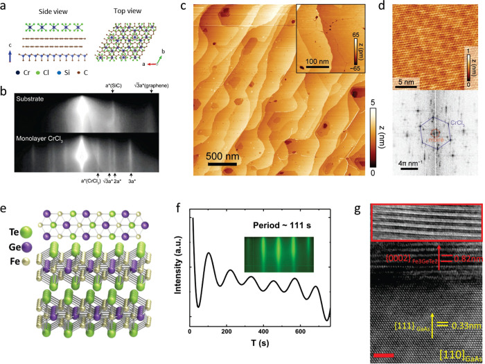
Figure 5.
Examples of large-area 2D magnets grown by MBE. (a–d) Monolayer CrCl3 on Graphene/SiC(0001) and (e–g) few-layer Fe3GeTe2 on GaAs (111). (a) Schematic crystal structure of CrCl3/graphene/6H-SiC layers in top-down view and cross-section view. (b) In situ RHEED pattern of the substrate and monolayer CrCl3 grown by MBE, along Γ–M of graphene (Γ–K of SiC). Streaks from different high-symmetry directions of CrCl3 are observed, implying a twisted in-plane orientation of the grains. (c) STM topography of a monolayer CrCl3 grown on graphene/6H-SiC(0001), indicating a homogeneous coverage on long length scales. Inset: A magnified topography image, which reveals the grain boundaries. (d) Atom resolved image of the CrCl3 lattice featuring a moiré pattern (upper panel) and its Fourier transformed image (lower panel). Panels (a–d) adapted with permission from ref (78). Copyright 2021 AAAS. (e) Crystal structure of Fe3GeTe2. (f) RHEED oscillations indicating layer-by-layer growth of Fe3GeTe2 (0001) on GaAs (111), and the corresponding electron diffraction pattern (inset). The inferred growth rate is 111 s per monolayer. (g) Transmission electron microscopy of a Fe3GeTe2/GaAs cross-section, indicating the (111)/(0002) epitaxial relationship. Panels (e–g) adapted with permission under a Creative Commins CC BY license from ref (99). Copyright 2017 Springer Nature.

