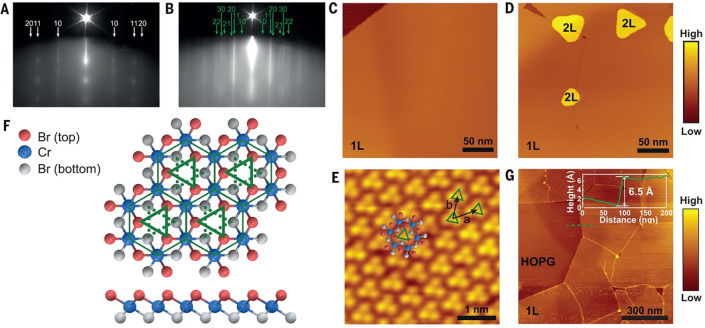
Figure 55.
(A, B) RHEED patterns with indicated diffraction orders of (A) the bare HOPG substrate and (B) the MBE-grown CrBr3 film. (C, D) STM images of (C) the CrBr3 monolayer with (D) bilayer islands. The scan parameters were as follows: Vb = 1.1 V, I = 100 pA, T = 5 K for (C) and Vb = 1.5 V, I = 100 pA, T = 5 K for (D). (E) Atomically resolved image of a monolayer CrBr3 with an overlaid atomic structure. The scan parameters were as follows: Vb = 1.5 V, I = 500 pA, T = 5 K. The lattice constants were determined to be 6.3 Å for the primitive vectors a and b, consistent with the bulk values. (F) Illustrations of the top and side views of the monolayer CrBr3 atomic structure. The Cr atoms form a honeycomb lattice sandwiched by Br atoms. Within the Cr honeycomb lattice, the top and bottom surfaces of Br atoms form single triangles but with opposite orientation, indicated by solid and dotted green lines, respectively. (G) AFM image of monolayer CrBr3 with partial coverage. A line-cut profile across the monolayer and bare substrate is shown with a monolayer height of 6.5 Å. All panels are adapted with permission from ref (20). Copyright 2019 AAAS.

