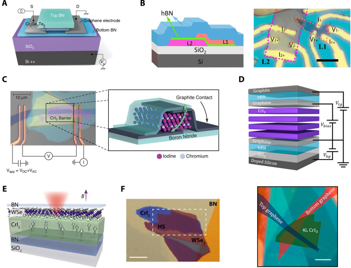
Figure 72.
Heterostructures fabricated from 2D vdW magnets. (A) Schematic of a Cr2Ge2Te6 flake fully encapsulated with hBN and contacted by graphene electrodes.10 Reproduced with permission from ref (10). Copyright 2018 Springer Nature. (B) Schematic (left) and corresponding optical image (right) of a MTJ fabricated from Fe3GeTe2 electrodes separated by an hBN barrier.109 In the right panel, the dotted lines outline the edges of the two Fe3GeTe2 flakes. The scale bar is 5 μm. Reproduced with permission from ref (109). Copyright 2018 American Chemical Society. (C) Optical image (left) and corresponding cartoon (right) of a spin-filter MTJ utilizing CrI3 as the tunnel barrier between graphene electrodes.14 Reproduced with permission from ref (14). Copyright 2018 AAAS. (D) Schematic (top) and a false-colored optical image (bottom) of a spin-field-effect transistor fabricated from 4-layer CrI3.504 Graphene acts as both transistor electrodes and local electrostatic gates. The scale bar is 5 μm. Reproduced with permission from ref (504). Copyright 2019 American Chemical Society. (E, F) Schematic (E) and false-colored optical image (F) of a heterostructure proximitizing CrI3 with WSe2.206 The scale bar in (F) is 5 μm. Panels (E, F) are reproduced with permission under Creative Commons CC BY-NC 4.0 license from ref (206). Copyright 2017 AAAS.

